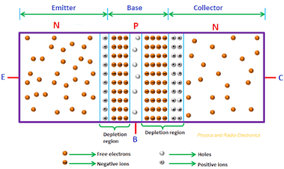
The construction and symbols of the p-n-p and n-p-n transistors is as shown in Figure respectively.
The important points about the construction of a transistor are as follows :
• The n-p-n transistor is formed by sandwiching a thin "p" type semiconductor between two "n" type semiconductors whereas a p-n-p transistor is formed by sandwiching a thin "n" type semiconductor between two p type semiconductors.
• In both the types, base comes in between collector and emitter region.
• Base is always a thin and lightly doped layer.
• Emitter and collector layers are much wider than the base and are heavily doped. To be precise, the emitter is the most heavily doped layer because it has to emit or inject electrons and the collector area is slightly larger than the emitter area. The collector area is largest because it is required to dissipate more heat.
• The transistor has two p-n junctions namely the collector base junction and base emitter junction.
 |
| Fig.Depletion Region In An Unbiased NPN Junction |
